
Printed Circuit Board Pictorial
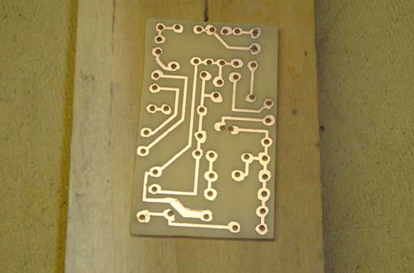
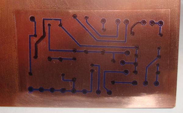
This pictorial describes how to create your own printed circuit board (PCB) using an "iron-on" transfer method. The image below is the "finished product" of this pictorial.
High Level Instructions
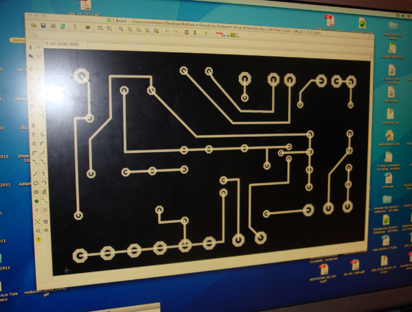
- DESIGN - design (or acquire) a PCB Layout. The circuit above is the prototype for the new Rothstein Guitars Overdrive pedal. The layout was designed using EAGLE software. If you are looking to create a PCB for an existing design, there are plenty of layouts available on the internet.
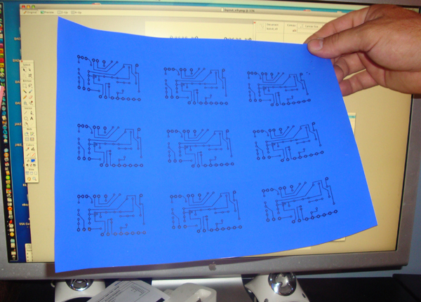
- PRINT - print the image onto transfer paper. We really like the Techniks Press-n-Peel Blue.
- PREPARE - prep the PCB blank by sanding/cleaning with steeel wool. Here is a list of tools I used for this pictorial:
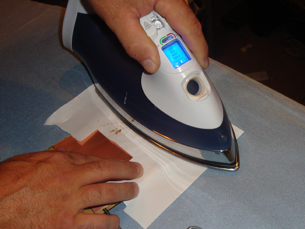
- TRANFER - apply heat via a common household iron for approximately 3-4 minutes to transfer the image to the PCB
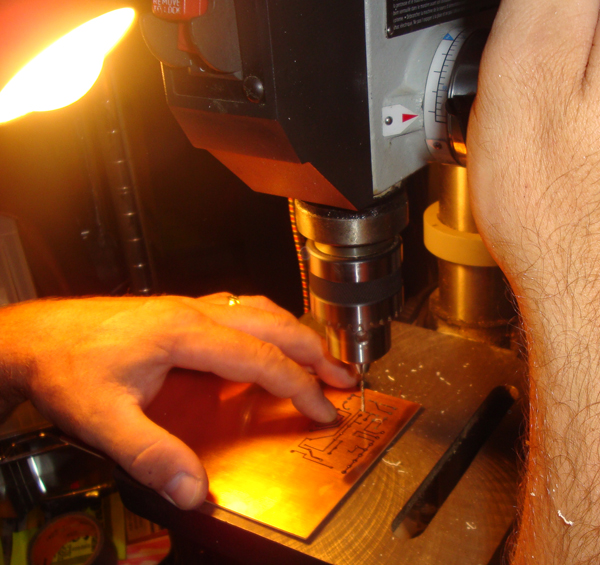
- DRILL - it is best to use a drill press to drill holes in the PCB for the components
- TOUCH UP - If you get any spots that are not dark enough, you may touch up either with a good sharpie pen.
- CUT DOWN TO SIZE
- ETCH - use etching solution available at Radio Shack (whch is Ferric Chloride) which will break down any of the copper not covered via the black ink.
- STEEL WOOL - Sand with steel wool to remove any black over the copper tracings
Tools used in this pictorial:
- Steel Wool
- Etchant Solution
- Copper clad board (PCB blank)
- Glass bowl
- Rubber Gloves
- Iron
- Transfer Paper (blue)
- Black Sharpie pen
We printed out several sheets.
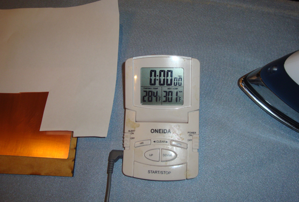
Heat an iron to the 275 - 325 range. We used a cooking thermometer to verify the temp of the iron.
Text.... Iron away for approximately 3 - 4 minutes. We prefer to cover the transfer paper with a layer of standard white paper.
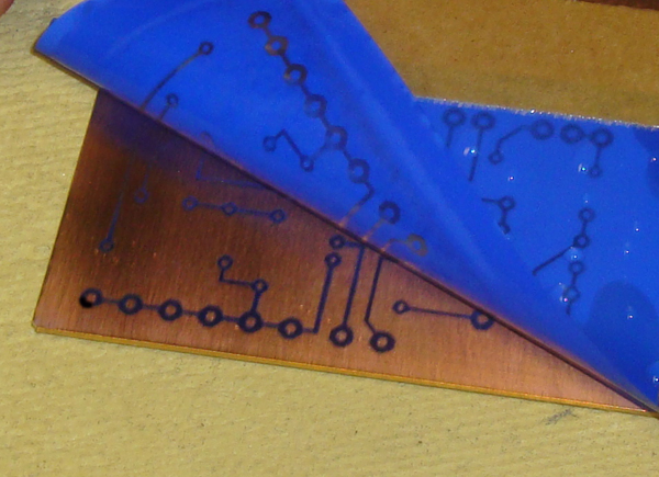
After getting "shocked" in a cold water bath the blue transfer paper is lifted
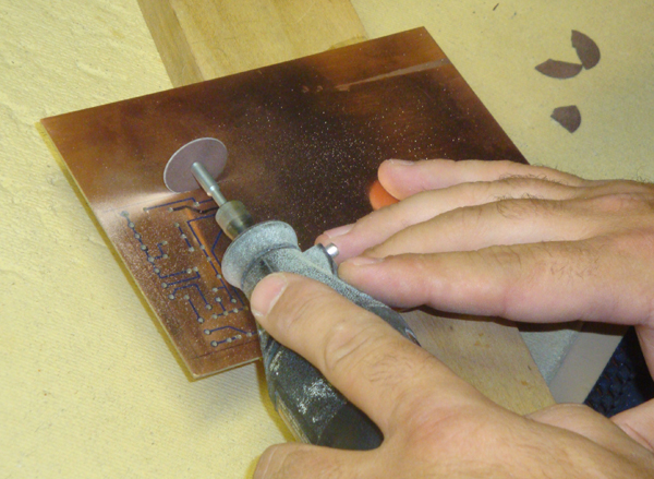
Next is time to drill out the holes. We prefer to use a drill press, however you may use a Dremel.
Any lines that do not appear dark enough, or any pads that are too small can be thickened simply by going over the area with a sharpie.
Cut down to size. We prefer to use a dremel for this.
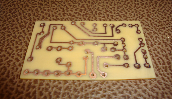
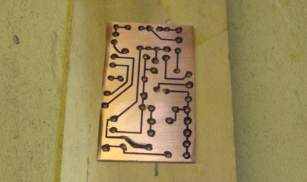
The PCB is now ready to get a bath in the etchant. All the black line and holes you see will resist the etchnat. Everything else will be removed by the etchant.
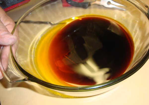
The PCB will require a 20 minute bath in the etchant solution. It is important to keep the solution moving which can be accomplished by gently rocking the bowl. Also make sure the solution is NOT cold. This should be done in a WELL VENTILATED AREA, and remember to wear rubber gloves and protective glasses.
There is a step that is not show. When the PCB is removed from the etchant, the traces wil all be black. You will need to sand again with steel wool to remove the black. After using the steel wool you will have something similar to what you see below.